

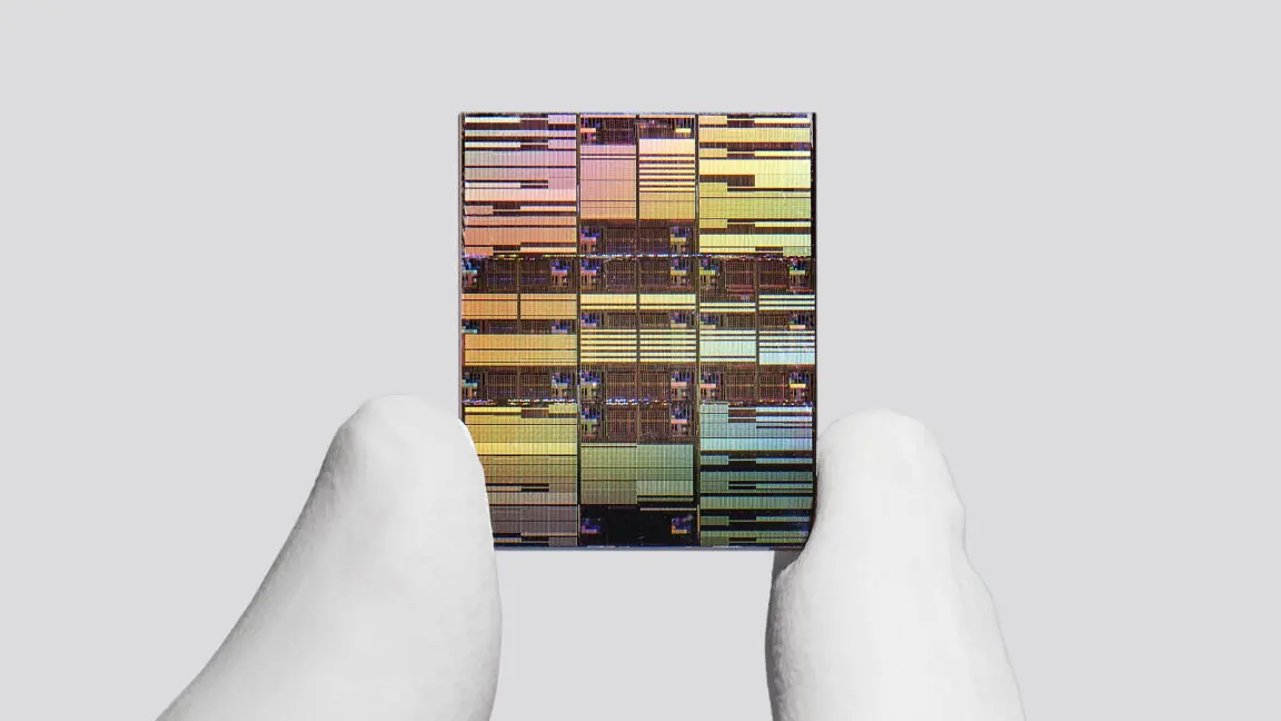
IBM has announced a breakthrough in semiconductor technology, claiming the world's first sub-1 nanometer chip architecture. The new design, called the nanostack, can integrate nearly 100 billion transistors on a chip the size of a human fingernail—almost twice the transistor density of the company's previous generation of chip technology. According to IBM, this leap will deliver dramatic improvements in computing performance and energy efficiency, specifically targeting the massive computational demands of AI data centers.
“It’s not just an incremental step, it’s a meaningful leap forward,” said Jay Gambetta, director of IBM Research, during an advance media briefing. He described the new technology as “pointing to a future where computing becomes significantly more powerful without a corresponding increase in energy.” The announcement was made at the 2025 IEEE Symposium on VLSI Technology and Circuits in Kyoto, Japan, where IBM researchers detailed the nanostack architecture and its potential.
The term “sub-1 nanometer” requires some clarification. It is practically impossible to build functional chips with physical features smaller than 1 nanometer due to quantum effects and fabrication limits. Instead, IBM uses the label to indicate that the new architecture delivers the performance improvements that would theoretically come from such tiny features. Specifically, IBM is calling this the 0.7-nanometer node, also referred to as the 7 angstrom node (since 1 nanometer equals 10 angstroms). However, these node numbers no longer correspond to actual gate lengths or feature sizes, a trend that has been true for decades. For example, the 3-nanometer and 2-nanometer chips currently in production have physical gate lengths much larger than their names suggest.
A New Architecture for Scaling
To overcome the physical scaling limits that have slowed Moore's Law, IBM engineers developed the nanostack architecture. Instead of shrinking transistors horizontally, this design stacks them vertically in a staggered layout, allowing more transistors to fit in the same chip area. The basic building block consists of two transistors stacked and bonded together. Each transistor contains three nanosheets, each 5 nanometers thick—equivalent to about 15 rows of silicon atoms—with a 9-nanometer gap between sheets.
This approach builds on IBM's earlier nanosheet transistor technology, which was introduced with its 2-nanometer node in 2021. Nanosheets have become the industry standard, adopted by leading foundries like TSMC for 3-nanometer and 2-nanometer chips. “Nanosheet has become the foundation of the next generation of transistor scaling,” said Huiming Bu, vice president of IBM Semiconductors Global R&D. According to Bu, the new nanostack will eventually replace nanosheet as the mainstream technology in advanced foundries.
Performance Gains for the AI Era
IBM projects that the nanostack architecture will enable a 50 percent increase in computing performance or a 70 percent improvement in energy efficiency compared to its 2-nanometer node. These gains come from the higher transistor density and improved electrical characteristics of the vertical design. In addition, IBM researchers demonstrated a 40 percent improvement in scaling for static random-access memory (SRAM) at the VLSI 2026 symposium. SRAM is critical for AI workloads because it provides fast, energy-intensive read and write operations. The improvement is achieved through a staggered-channel design for the SRAM bit cells (six-transistor memory units), which reduces cell height by 40 percent and allows more SRAM to fit in the same space.
This is welcome news for AI chip designers, as SRAM scaling had stagnated in recent generations. Between the 3-nanometer and 2-nanometer nodes, SRAM scaling improved by only a few percent. “This achievement of 40 percent will eventually industrialize itself in AI workflows, which require higher bandwidth and high efficiency,” Gambetta explained. The improvements are expected to benefit both central processing units (CPUs) and graphics processing units (GPUs) used in AI data centers.
Historical Context and Industry Impact
The semiconductor industry has long relied on shrinking transistor dimensions to improve performance and reduce costs, following Moore's Law. However, as physical limits approach, alternative approaches like vertical stacking, new materials, and advanced packaging have become essential. IBM has been at the forefront of such innovations for decades, pioneering technologies like copper interconnects, silicon-on-insulator, and high-k metal gates. The nanostack architecture is the latest in this lineage.
Other companies are also exploring vertical transistor designs. For instance, Intel has introduced RibbonFET, a gate-all-around (GAA) transistor, for its 20A node. Samsung and TSMC are developing their own GAA technologies. However, IBM claims its nanostack goes beyond traditional GAA by stacking multiple transistors vertically, rather than just folding the gate around a single nanosheet. This distinction is key to achieving the claimed density and performance gains.
IBM is primarily a research lab and does not manufacture its own chips at scale. Instead, it commercializes its technologies through partnerships. For the 2-nanometer node, IBM collaborated with Rapidus in Japan and Samsung in South Korea. The company declined to name partners for the new sub-1 nanometer node, but executives expect commercial chips to start production within five to ten years. “It will replace nanosheet as today’s mainstream in leading foundries, whether it’s CPUs or GPUs,” Bu said. “Within a decade, this will become another mainstream that we have invented and helped industry to transform.”
The implications for AI are significant. Current AI models require enormous computational power and energy. The nanostack's improvements could reduce the carbon footprint of training and inference, while enabling more complex models. Moreover, the SRAM scaling benefit directly addresses the memory bottleneck that often limits AI performance. With faster, denser memory, chips can process data more efficiently, reducing the need to access slower external memory.
Looking ahead, the race to sub-1 nanometer equivalents is heating up. TSMC is reportedly working on 1.4-nanometer technology, while Intel aims to lead with 18A by 2026. IBM's announcement, though not a product, establishes a benchmark for what is possible. The company has a track record of demonstrating technologies years before they reach market—its 2-nanometer nanosheet technology was announced in 2021 and is now being commercialized by partners. Similarly, the nanostack could influence the next decade of chip design.
Researchers also see applications beyond digital logic. The vertical stacking approach could be adapted for analog, radio-frequency, and memory devices, potentially enabling fully integrated systems-on-chip. This would align with the industry trend toward heterogeneous integration, where different function blocks are combined in a single package.
In summary, IBM has laid out a clear roadmap for continuing transistor scaling beyond conventional limits. By focusing on architecture rather than pure lithography, the company offers a path to continue reaping the benefits of Moore's Law in the AI era. The nanostack may not be the only approach, but it represents a significant step forward, with concrete performance predictions and a plausible commercialization timeline. As industry partners evaluate the technology, the next five years will determine whether IBM's latest invention becomes as transformative as its past breakthroughs.
Source: Ars Technica News